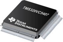
●This data manual discusses features and specifications of the TMS320VC5407 and TMS320VC5404 (hereafter referred to as the 5407/5404 unless otherwise specified) digital signal processors (DSPs). The 5407 and 5404 are essentially the same device except for differences in their memory maps.
●This section lists the pin assignments and describes the function of each pin. This data manual also provides a detailed description section, electrical specifications, parameter measurement information, and mechanical data about the available packaging.
●NOTE: This data sheet is designed to be used in conjunction with the _TMS320C5000 DSP Family Functional Overview_ (literature number SPRU307).
●The 5407/5404 are based on an advanced modified Harvard architecture that has one program memory bus and three data memory buses. These processors provide an arithmetic logic unit (ALU) with a high degree of parallelism, application-specific hardware logic, on-chip memory, and additional on-chip peripherals. The basis of the operational flexibility and speed of these DSPs is a highly specialized instruction set.
●Separate program and data spaces allow simultaneous access to program instructions and data, providing a high degree of parallelism. Two read operations and one write operation can be performed in a single cycle. Instructions with parallel store and application-specific instructions can fully utilize this architecture. In addition, data can be transferred between data and program spaces. Such parallelism supports a powerful set of arithmetic, logic, and bit-manipulation operations that can all be performed in a single machine cycle. These DSPs also include the control mechanisms to manage interrupts, repeated operations, and function calls.
● Advanced Multibus Architecture With Three Separate 16-Bit Data Memory Buses and One Program Memory Bus
● 40-Bit Arithmetic Logic Unit (ALU) Including a 40-Bit Barrel Shifter and Two Independent 40-Bit Accumulators
● 17- × 17-Bit Parallel Multiplier Coupled to a 40-Bit Dedicated Adder for Non-Pipelined Single-Cycle Multiply/Accumulate (MAC) Operation
● Compare, Select, and Store Unit (CSSU) for the Add/Compare Selection of the Viterbi Operator
● Exponent Encoder to Compute an Exponent Value of a 40-Bit Accumulator Value in a Single Cycle
● Two Address Generators With Eight Auxiliary Registers and Two Auxiliary Register Arithmetic Units (ARAUs)
● Data Bus With a Bus Holder Feature
● Extended Addressing Mode for 8M × 16-Bit Maximum Addressable External Program Space
● On-Chip ROM
● 128K × 16-Bit (5407) Configured for Program Memory
● 64K × 16-Bit (5404) Configured for Program Memory
● On-Chip RAM
● 40K × 16-Bit (5407) Composed of Five Blocks of 8K × 16-Bit On-Chip Dual-Access Program/Data RAM
● 16K x 16-Bit (5404) Composed of Two Blocks of 8K × 16-Bit On-Chip Dual-Access Program/Data RAM
● Enhanced External Parallel Interface (XIO2)
● Single-Instruction-Repeat and Block-Repeat Operations for Program Code
● Block-Memory-Move Instructions for Better Program and Data Management
● Instructions With a 32-Bit Long Word Operand
● Instructions With Two- or Three-Operand Reads
● Arithmetic Instructions With Parallel Store and Parallel Load
● Conditional Store Instructions
● Fast Return From Interrupt
● On-Chip Peripherals
● Software-Programmable Wait-State Generator and Programmable Bank-Switching
● On-Chip Programmable Phase-Locked Loop (PLL) Clock Generator With External Clock Source
● Two 16-Bit Timers
● Six-Channel Direct Memory Access (DMA) Controller
● Three Multichannel Buffered Serial Ports (McBSPs)
● 8/16-Bit Enhanced Parallel Host-Port Interface (HPI8/16)
● Universal Asynchronous Receiver/Transmitter (UART) With Integrated Baud Rate Generator
● Power Consumption Control With IDLE1, IDLE2, and IDLE3 Instructions With Power-Down Modes
● CLKOUT Off Control to Disable CLKOUT
● On-Chip Scan-Based Emulation Logic, IEEE Std 1149.1 (JTAG) Boundary Scan Logic
● 144-Pin Ball Grid Array (BGA) (GGU Suffix)
● 144-Pin Low-Profile Quad Flatpack (LQFP) (PGE Suffix)
● 8.33-ns Single-Cycle Fixed-Point Instruction Execution Time (120 MIPS)
● 3.3-V I/O Supply Voltage
● 1.5-V Core Supply Voltage
●IEEE Standard 1149.1-1990 Standard-Test-Access Port and Boundary Scan Architecture.
●All trademarks are the property of their respective owners.
●TMS320C54x is a trademark of Texas Instruments.
 Part 3D Model