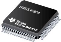
●The DS92LV090A is one in a series of Bus LVDS transceivers designed specifically for the high speed, low power proprietary backplane or cable interfaces. The device operates from a single 3.3V power supply and includes nine differential line drivers and nine receivers. To minimize bus loading, the driver outputs and receiver inputs are internally connected. The separate I/O of the logic side allows for loop back support. The device also features a flow through pin out which allows easy PCB routing for short stubs between its pins and the connector.
●The driver translates 3V TTL levels (single-ended) to differential Bus LVDS (BLVDS) output levels. This allows for high speed operation, while consuming minimal power with reduced EMI. In addition, the differential signaling provides common mode noise rejection of ±1V.
●The receiver threshold is less than ±100 mV over a ±1V common mode range and translates the differential Bus LVDS to standard (TTL/CMOS) levels. (See Section for more details.)
● Bus LVDS Signaling
● 3.2 Nanosecond Propagation Delay Max
● Chip to Chip Skew ±800ps
● Low Power CMOS Design
● High Signaling Rate Capability (Above 100 Mbps)
● 0.1V to 2.3V Common Mode Range for VID = 200mV
● ±100 mV Receiver Sensitivity
● Supports Open and Terminated Failsafe on Port Pins
● 3.3V Operation
● Glitch Free Power Up/Down (Driver & Receiver Disabled)
● Light Bus Loading (5 pF Typical) per Bus LVDS Load
● Designed for Double Termination Applications
● Balanced Output Impedance
● Product Offered in 64 Pin LQFP Package
● High Impedance Bus Pins on Power off (VCC = 0V)
● Driver Channel to Channel Skew (Same Device) 230ps Typical
● Receiver Channel to Channel Skew (Same Device) 370ps Typical
●All trademarks are the property of their respective owners.

 Part 3D Model
