●Overview
●The CBTL05023 is a multiplexer/demultiplexer switch chip for DisplayPort v1.2 signals and the control signals of a 10 Gbit/s channel. The 10 Gbit/s channel does not pass through this switch. This chip provides BIASOUT output control signal, and the DC-biasing pull-down resistors to facilitate an external 10 Gbit/s channel.
●The AUX MUX is a 2 : 1 switch with CA_DETect pin selecting between AUX and DDC (Direct Display Control) signals.
●The DP MUX is a 2 : 1 switch that selects between DPML (DisplayPort Main Link) and LSTX/LSRX signals.
●This chip also includes three control signal buffers: HPDOUT, CA_DETOUT and BIASOUT.
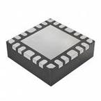
●CBTL05023 is powered by a 3.3 V supply and it is available in 3 mm x 3 mm HVQFN24 package with 0.4 mm pitch.
●MoreLess
●## Features
●### AUX MUX 2 : 1 switch
● This 2 : 1 switch is controlled by CA_DET signal multiplexing of the 1 Mbit/s differential AUX and DDC (Direct Display Control) signals
● When CA_DET is HIGH, DDC path is selected
● Differential AUX channel:
● Low insertion loss: -0.5 dB at 5 MHz
● Low return loss: -19 dB at 5 MHz
● Low ON-state resistance: 7.5 Ω
● Bandwidth: 5 GHz
● Low off-state isolation: -75 dB at 5 MHz
● Low crosstalk: -40 dB at 5 MHz
● Common-mode input voltage VIC: 0 V to 3.3 V
● Differential input voltage VID: 1.4 V (maximum)
● DDC channel has DDC_CLK and DDC_DAT I²C signals
● 100 kHz 3.3 V voltage swing
● Both AUXIO+ and AUXIO- outputs have 900 Ω (±20 %) pull-down resistor that is enabled by the status of the BIASOUT output pin
● These pull-down resistors provide DC bias for the 10 Gbit/s channel
●### DP MUX 2 : 1 switch
●The DP MUX is a 2:1 switch that is controlled by DP_PD pin multiplexing of a differential DPML signal and LSTX/LSRX signals
● The DPML (DisplayPort Main Link) runs up to HBR2 data rate of 5.4 Gbit/s
● The low speed DC coupled signals LSTX and LSRX are 3.3 V single-ended signals that operated at 1 Mbit/s
● 5.4 Gbit/s DPML channel:
● Low insertion loss for DP-DPMLO path: -2.0 dB at 2.5 GHz
● Low insertion loss for LS-DPMLO path: -2.0 dB at 2.5 GHz
● Low return loss for DP-DPMLO path: -15 dB at 2.5 GHz
● Low return loss for LS-DPMLO path: -14 dB at 2.5 GHz
● Low ON-state resistance for DP-DPMLO path: 9 Ω
● Low ON-state resistance for LS-DPMLO path: 13 Ω
● High bandwidth: 7 GHz
● Low off-state isolation: -20 dB at 2.5 GHz
● Low crosstalk: -25 dB at 2.5 GHz
●### General
● The input of the HPDOUT (Hot Plug Detect output) buffer is 5 V tolerant
● HPDOUT, CA_DETOUT and BIASOUT buffers
● CA_DET input leakage current < 0.1 μA to prevent driving the 1 MΩ pull-down to a HIGH level
● BIASOUT buffer is able to provide enough current to drive the bias circuit for the PIN diode path
● BIASOUT buffer can drive up to six sets of bias circuits for the 10 Gbit/s paths
● When AUXIO_EN is LOW or (BIASIN = 0 and DP_PD = 1), this chip is in Sleep mode
● AUXIO+ and AUXIO- of AUX MUX are disabled
● CA_DETOUT and HPDOUT buffers are on
● When the chip is in Sleep mode, CBTL05023 will consume < 3.5 mW
● Patent-pending high-bandwidth analog pass-gate technology
● Very low intra-pair differential skew (5 ps typical)
● All channels have back current protection
● All channels support rail-to-rail input voltage
● CMOS input buffer with hysteresis
● Single 3.3 V ± 10 % power supply
● HVQFN24 3 mm x 3 mm package, 0.4 mm pitch, with exposed center pad for thermal relief and electrical ground
● ESD: 2500 V HBM, 1250 V CDM
● Operating temperature range: 0 °C to 85 °C
●## Features