●Product Details
●The ADN2811 provides the receiver functions of quantization, signal level detect, and clock and data recovery at OC-48 and OC-48 FEC rates. All SONET jitter requirements are met, including jitter transfer, jitter generation, and jitter tolerance. All specifications are quoted for −40°C to +85°C ambient temperature, unless otherwise noted.
●The device is intended for WDM system applications and can be used with either an external reference clock or an on-chip oscillator with external crystal. Both the 2.48 Gbps and 2.66 Gbps digital wrapper rates are supported by the ADN2811, without any change of reference clock.
●This device, together with a PIN diode and a TIA preamplifier, can implement a highly integrated, low cost, low power, fiber optic receiver.
●The receiver front end signal detect circuit indicates when the input signal level has fallen below a user-adjustable threshold. The signal detect circuit has hysteresis to prevent chatter at the output.
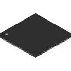
●The ADN2811 is available in a compact, 7 mm × 7 mm, 48-lead chip scale package.
●Applications
● SONET OC-48, SDH STM-16, and 15/14 FEC
● WDM transponders
● Regenerators/repeaters
● Test equipment
● Backplane applications
●### Features and Benefits
● Meets SONET requirements for jitter transfer/generation/tolerance
● Quantizer sensitivity: 4 mV typical
● Adjustable slice level: ±100 mV
● 1.9 GHz minimum bandwidth
● Patented clock recovery architecture
● Loss of signal detect range: 3 mV to 15 mV
● Single reference clock frequency for both native SONET and 15/14 (7%) wrapper rate
● Choice of 19.44 MHz, 38.88 MHz, 77.76 MHz, or 155.52 MHz REFCLK
● LVPECL/LVDS/LVCMOS/LVTTL compatible inputs (LVPECL/LVDS only at 155.52 MHz)
● 19.44 MHz on-chip oscillator to be used with external crystal
● Loss of lock indicator
● Loopback mode for high speed test data
● Output squelch and bypass features
● Single-supply operation: 3.3 V
● Low power: 540 mW typical
● 7 mm × 7 mm, 48-lead LFCSP